


In today’s landscape, the advent of custom wafer solutions has taken over the world. These solutions are reshaping the way industries operate. This is especially true in the semiconductor industry.
So, in this case study, we delve into the transformative role of custom wafer solutions. We will explore its impact on operational efficiency, innovation, and productivity. Let’s begin.
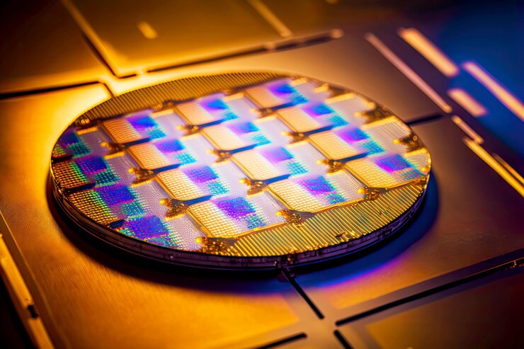
What Are Custom Wafer Solutions?
Custom wafer solutions are the cutting-edge approach in the field of semiconductor industry. Wafers meet the specific needs of individual clients. These wafers are thin slices of semiconductor material such as silicon. They are the foundation for integrated circuits.
Customization may involve varying the wafers’:
- size
- material
- thickness
- doping properties
- layout
- circuit design
This enables manufacturers to optimize the performance and efficiency of their electronic devices. Whatever a project needs, there’s a wafer solution for exactly that.
These wafers, like the ones by https://www.silybwafers.com/, can fit any project requirements. This drives innovation while maximizing operational efficiency.
How Are They Made?
The process of creating wafer solutions is complex. It involves a series of steps. Each step is critical in achieving the desired characteristics of the wafer.
The first step involves growing a single crystal from molten silicon using a process called Czochralski (CZ) method. Once the crystal is grown, it is then sliced into thin wafers using a diamond saw. The next step involves polishing and cleaning the wafer to remove any impurities.
After that, the wafer is doped with specific materials to create regions of different electrical properties, which are used to form integrated circuits.
Lastly, a thin layer of photoresist is applied on top of the wafer. This layer is then exposed to light through a photomask, which transfers the circuit design onto the wafer. The exposed areas are then etched away to reveal the final product – a customized wafer solution.
The Advantages
Wafer solutions have many benefits for different projects. Some of these advantages are the following:
Increased Efficiency
Different custom solutions have specific applications. This means that they can deliver better efficiency compared to generic wafers. This is crucial in industries where small things can make a significant difference.
Cost Savings
While custom solutions may have a higher initial cost, they can lead to long-term cost savings. These solutions can help businesses reduce energy consumption and cut waste. This translates into significant cost savings over the product’s lifespan.
Greater Precision
Custom solutions allow for great precision in the production of integrated circuits. Manufacturers can achieve a high level of detail and specificity. This enhances the performance of the final product.
Boosting Innovation
Custom wafer solutions are driving innovation across industries. They can pave the way for the exploration of new methodologies and technologies. This is because they provide the flexibility to experiment with different designs. This flexibility encourages creative problem-solving and paves the way for breakthroughs in microelectronics.
Improved Product Lifecycle
With the ability to tailor wafers, custom solutions can extend the product lifecycle. The efficiency of devices that use custom wafers can lead to longer-lasting equipment. They will need less frequent replacement, thereby contributing to sustainability efforts.
Real-World Examples
Custom wafer solutions have already made a significant impact in industries such as:
- healthcare
- aerospace
- solar energy
- telecommunications
- automotive
In the healthcare sector, custom wafers help develop advanced diagnostic and monitoring devices. This includes glucose monitors for diabetes management and wearable sensors for patient monitoring.
In the aerospace industry, these solutions enable the development of high-performance components. This not only improves fuel efficiency but also enhances safety and reliability.
In the solar energy sector, wafer solutions play an instrumental role. Photovoltaic (PV) cells are composed of semiconductor materials like silicon. By customizing the wafers used in cells, manufacturers can optimize the cells’ efficiency. This can lead to more cost-effective and efficient solar panels.
The telecommunications industry is another arena seeing the benefits of customized wafer solutions. In the production of devices for 5G networks, generic wafers may not be up to par. Custom wafers can have precise material properties needed to support 5G frequencies. This can enable faster, more reliable data transmission.
In the automotive industry, wafers help in creating better electric vehicles (EVs). Power electronics are critical for controlling and converting electrical energy in EVs. And they rely on semiconductor devices.
Custom wafers allow for the development of semiconductors that can withstand high voltages. They can also withstand temperatures encountered in EVs, improving the vehicles’ performance.
Across industries, custom solutions are paving the way for innovative applications. They are pushing for higher efficiency and cost savings. So, they have become a significant enabler in the world of technology.
The Future Of Custom Wafer Solutions
The trajectory of customized wafer solutions is bright and promising. Technological advancements are likely to further refine the customization process. This enables even greater precision and efficiency.
The integration of AI and machine learning technologies could also occur. This can promote smarter, adaptive manufacturing processes. So they can better respond to unique project needs in real time.
Moreover, people will continue to discover and harness new semiconductor materials. So, we may witness the development of wafer technology with unprecedented capabilities. These solutions could offer enhanced performance, durability, and energy efficiency. It could push the boundaries of what’s currently achievable in microelectronics.
There is also the rising trend of miniaturization in electronics. This can spur further growth in the demand for customized wafer solutions.
Innovations in wafer-level packaging are also expected. This includes the development of more cost-effective, reliable, and compact packaging solutions. With the global push towards sustainability, sustainable practices will also be the norm.
Industries like 5G communications will also continue to expand. So they will likely fuel the need for high-quality, bespoke wafers.
In essence, custom wafer solutions will play a pivotal role in the future of technology. They will enable groundbreaking innovations and drive efficiency across sectors.
Wafer Technology Is the Future
Custom wafer solutions are revolutionizing the world by fostering innovation. They are contributing to long-term cost savings across a wide array of industries.
The future of these solutions is bright. Custom wafer solutions stand as a testament to the potential of manufacturing.
Did you find this article helpful? If so, check out the rest of our site for more.
Read Also: